I2S Audio Codec Interface with STM32H743

Interfacing an audio codec with a microcontroller is a common task in DSP and audio-related projects.
This post will summarize the basics steps that have to be taken in order to make an audio codec work with an STM32 microcontroller.
Most of the principles exposed here can be applied to any audio codec which uses i2s protocol and control registers for hardware configuration.
Introduction
In this case, the audio codec will be the WM8960, form Cirrus Electronics.
As a brief explanation, this piece of hardware is an integrated circuit with multiple features which allow the user to build a high-quality interface between continuous and discrete audio signals, bith forward and backwards.
Basically, its main purpose is receiving (encoding) audio signals and converting it to a data stream while, simultaneously, converting from digital to analog (decoding). Both tasks are done by using i2s protocol.
This i2s interface can be configured to meet specific project requirements as the sampling frequency, channel/pinout routing, muting/unmuting, power modes etc. For this IC, this configuration is made via i2c registers, adressing its integrated control interface.
In some other audio codecs which, usually are more simple, this configuration is done by setting certain pins at specific logic levels (High/Low).
The main benefit for having a dedicated control interface inside the audio codec is that it gives a vastly greater configuration of the internal features.
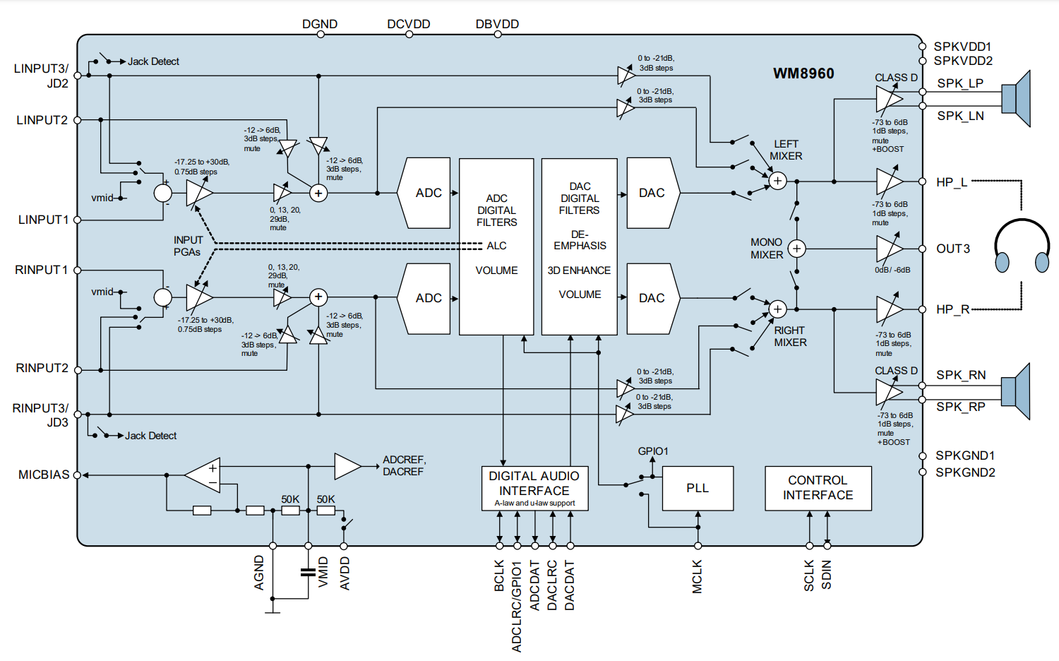
As can be seen in the block diagram, there are multiple processing and routing blocks embedded inside the IC.
Although it is possible to change the internal configuration while the program is actually running, the essential step that need to be taken is configuring its features when initializing the device.
That said, this could be a basic flow diagram of its configuration proccess.
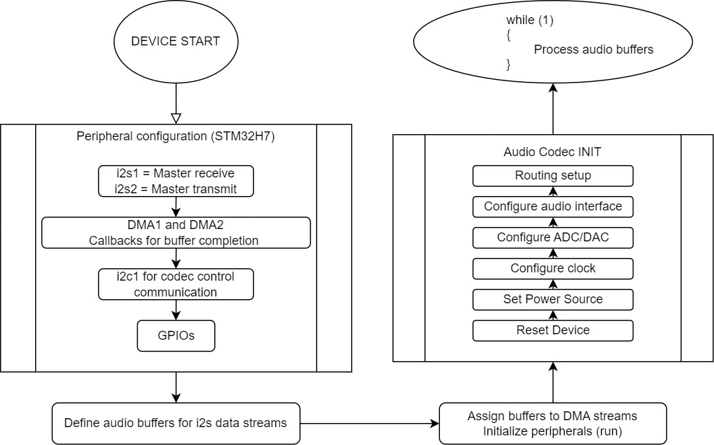
With this diagram, it is easy to know what must be done first, configuring the microcontroller’s peripherals.
Peripheral configuration
In every microcontroller, the different peripherals are configured using registers that are explained in detail in the manufacturer’s datasheet.
Doing this manually can be a very slow proccess, specially when you are new to a certain platform like, for instance, the c2000 MCUs from Texas Instruments.
STMicroelectronics, on the other hand, has developed a framework to ease the programming of their MCUs.
This framework is based on a code generator and a hardware abstraction layer (HAL). In this project, both tools will be used during the peripheral configuration.
i2s and DMA
We want our MCU to continuously receive and send digital audio streams in combination with the audio codec. To do so, the DMA will need to be set as well.
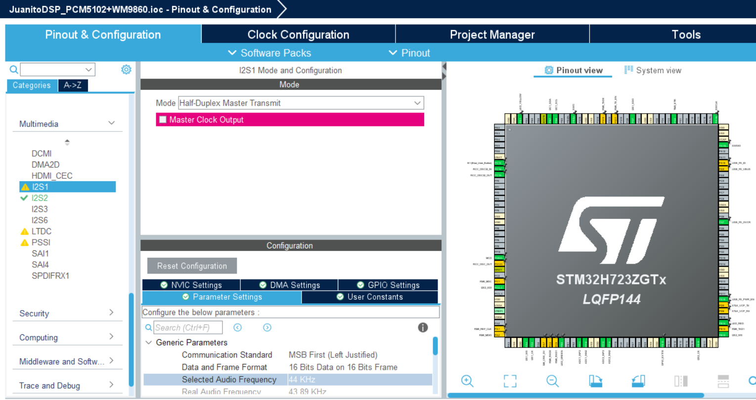
Basically, these are the important configuration parameters in the i2s1 (transmitter):
Parameter settings:
- Mode: Half-Duplex Master Transmit
- Comunication Standard: MSB First (Left Justified)
- Data and Frame Format: 16 bits on 16 Bits Frame
- Selected audio frequency: 44KHz (This is optional)
DMA settings: Add a DMA request (SPI1_TX, for example)
- Stream: DMA1 Stream 1
- Direction: Memory To Peripheral
GPIO Settings: We have three signals in the i2s protocol:
- I2S1_WS (Word select, best known as LeftRightClock)
- I2S1_CK (Clock)
- I2S1_SDO (Data output)
A physical pin of the MCU needs to be assigned to every signal individually. This is personal and the best option is always to make a decision based on the layout of the PCB. This can be changed anytime.
For the receiver, another independent i2s needs to be configured. In this case, it will be the i2s. The configuration is almost identical, the only different parameters are those:
Transmitter settings:
- In parameter settings, mode must be Half-Duplex Master Receive
- We need to add another independent DMA request, so the DMA stream must be different. For example, DMA1 Stream 2
NVIC Settings
In order to make a callback function that sets the synchronism between the processing and reading states of the system, the NVIC settings must be configured. We need to add an interrupt routine for each DMA stream, one for each i2s channel.
i2c
It is not necesary to change much of the settings here, but it is important to check a few things:
Parameter settings:
- Primary Adress Length: 7-bit
- Dual Adress Aknowledged: Disabled
GPIO Setings: The i2c protocol uses two wires to communicate. They need to be assigned to physical pins.
- I2C1_SCL (Clock)
- I2C1_SDA (Data, bidirectional)
Define audio buffers for i2s data streams
At this time, we need to define some buffers that will store the audio samples before and after the processing.
Beginning of main.c:
|
|
This processing flag will be set to 1 when the audio input buffer is half completed and full completed. The reason for this is to proccess the half of the buffer that has already been filled while the other half is being filled.
This technique is called Ping-Pong Buffering, and it is intended to ensure that the processing is sinchronized with the ADC and DAC conversions.
This function will be covered later.
Start Peripherals
Now, each peripheral needs to be initialized.
All those “Init” functions were written by the code generator, and they basically set the registers needed to match the configuration that has been decided before.
int main(void) function of main.c:
|
|
Audio codec INIT
This function is responsible of writting all the registers needed in order to configure all the operation modes desired for the audio codec.
The register is written by calling the function WM8960_Write_Reg(reg, dat) where, “reg” is the register address that corresponds to an specific register and, “dat” is the actual value that is being written in that address.
All the addresses are referenced in the manufacturer’s datashet, as well as the possible configurations that we can write in the “dat” argument.
WM8960_init() function of main.c:
|
|
WM8960_Write_Reg() function of main.c:
|
|
WM8960_ReadReg() function of main.c:
|
|
Buffer completion callbacks
Each of the two functions are intended to do two different tasks. The first one is changing the pointers loctaion to the position of the buffer that needs to be processed later. The second one is setting the DataReadyFlag to 1 so that the processing can start after the callback is finished.
HAL_I2SEx_TxRxHalfCpltCallback(I2S_HandleTypeDef *hi2s) function in main.c:
|
|
HAL_I2SEx_TxRxCpltCallback(I2S_HandleTypeDef *hi2s) function in main.c:
|
|
Infinite loop
This is the infinite loop. All the processing must be done here, by calling the Process_Data() function, where there will be one independent function for each filter that has to be executed.
while(1) function in main.c:
|
|
This function is intended to proccess half of the buffer each time is called. This is done to work with the Ping-Pong Buffering technique that was introduced earlier.
Once the proccessing is done, the DataReadyFlag is set to 0. This flag will remain in this state until it occurs a callback whenever the new half of the buffer has been filled, meaning that, again, it is time to proccess.
Process_Data() function in main.c:
|
|