STM32 DSP Framework for Audio Applications

Introduction
This project aims to create an intuitive, modular, and efficient platform with a focus on advanced DSP techniques and connectivity options for real-time DSP-based audio product development. With its high flexibility, this platform empowers the creation of more complex projects such as portable speakers, synthesizers, and noise cancelling systems.
The objective is to create an industry-standard platform which will allow my future projects to reach the technology level of the most powerful audio products in the market.
I will explore various disciplines, including advanced DSP techniques for audio, communication protocols, buffering, data streaming, hardware design, and software optimization for power efficiency.
The system can be described as a microcontroller-based solution designed to handle both digital and analog audio inputs which is capable of processing the audio sources using customizable DSP algorithms.
The PCB itself must include the peripherals and connectors needed in order to meet the next connectivity requirements:
- Bluetooth A2DP, aptX.
- Line input
- Preamplified input (for instruments)
- Stereo Line output
- Stereo auxiliar output (for 2.1 speaker systems for example)
- Battery connection
- USB connection for external programming and/or charging the battery
The device must be able to disable some of these peripherals in case that they are not being used as a way to reduce the power consumption of future projects.
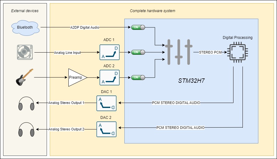
Block diagram
This is the block diagram of the system. The yellow rectangle represents the whole hardware device, including the microcontroller and the ICs that are used for A/D and D/A conversion. The blue rectangle in the center represents the microcontroller, and every block inside it consists of digital algorithms and communication protocols.
Hardware overview
The hardware components are the following:
- Bluetooth receiver
- 2x Stereo ADCs
- 2x Stereo DACs
- Preamplification circuit
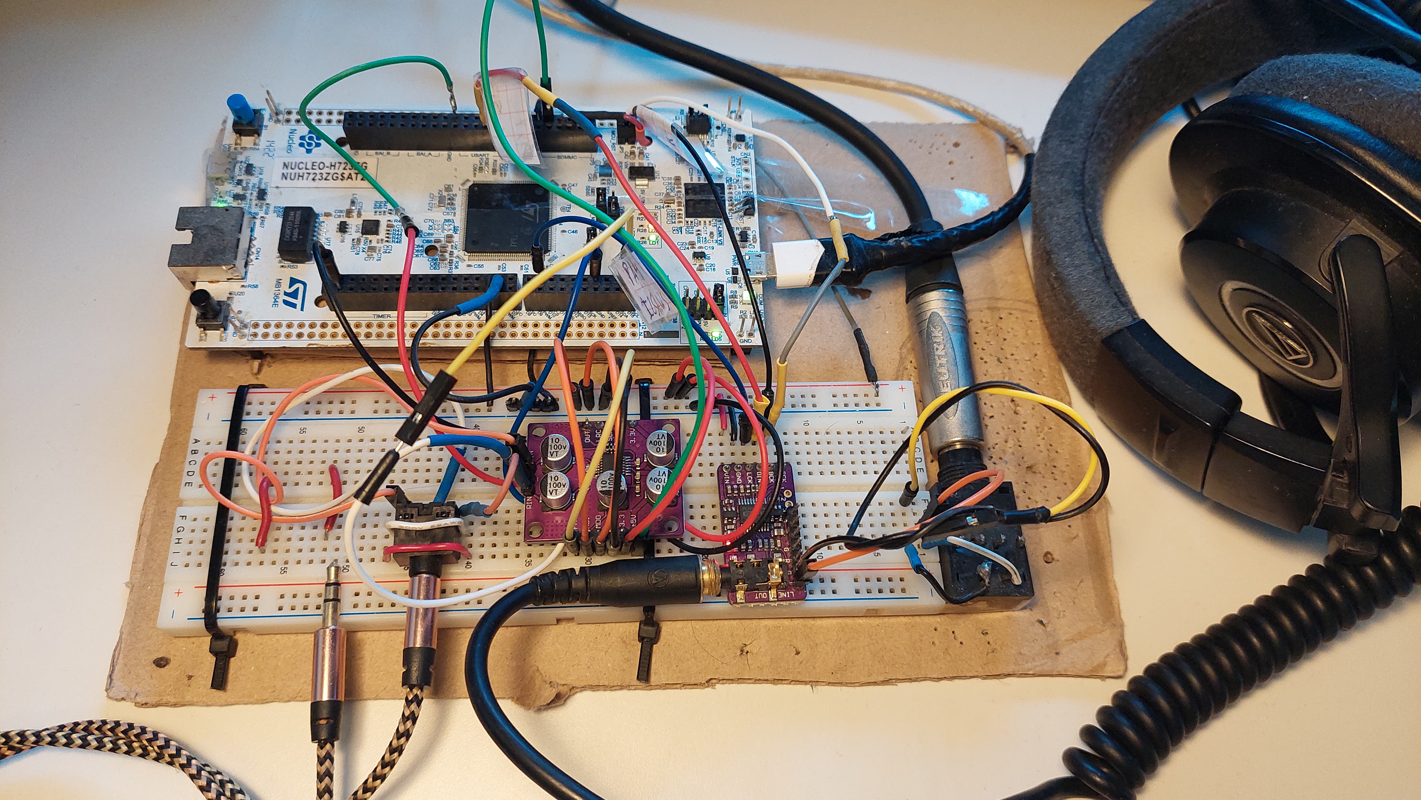
This is how the system looks at this point. Each part will be explained in more depth below.
A/D Converters
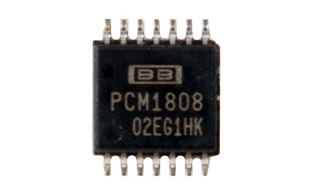
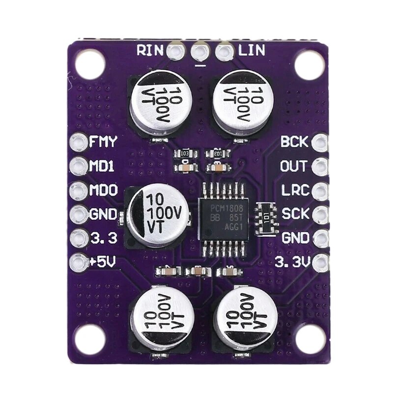
The chosen IC for A/D conversion is the PCM1808 from Texas Instruments.
It is a Single-Ended stereo ADC that operates at 24 bits and a samling frequency that ranges from 44.1 to 96 KHz depending on the clock configuration. It streams the converted audio using the I2S protocol. It has some built-in features that ensure good sound quality, such as:
- Oversampling Decimation Filter, useful to prevent aliasing noise
- On-Chip Analog Low-Pass Filter
- On-Chip High-Pass Filter
- Power Down and Reset System
- Configurable I2S format
BLOCK DIAGRAM
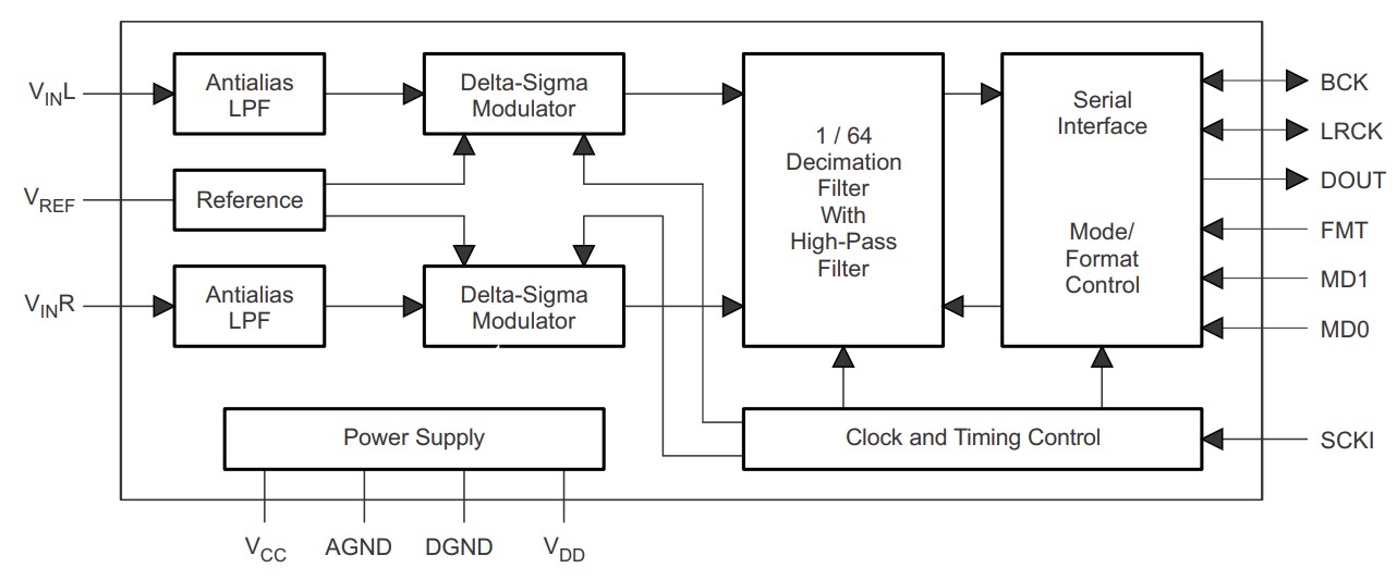
In order to make these added features work, it also needs to be fed with a higher frequency System Clock, which has to be synchronized with the rest of the I2S signals.
Eventhough a full-system mixed-signal PCB will be designed in the future, This IC is also available in a development board which comes very handy for the early stages of the project. This is the development board that has been implemented in the system at this moment:
D/A Converters
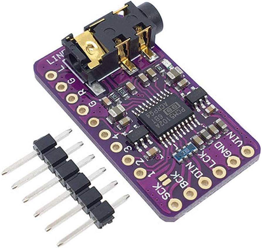
The digital to analog conversion will be done by using a very simple but effective IC that I already used on past projects, the PCM5102.
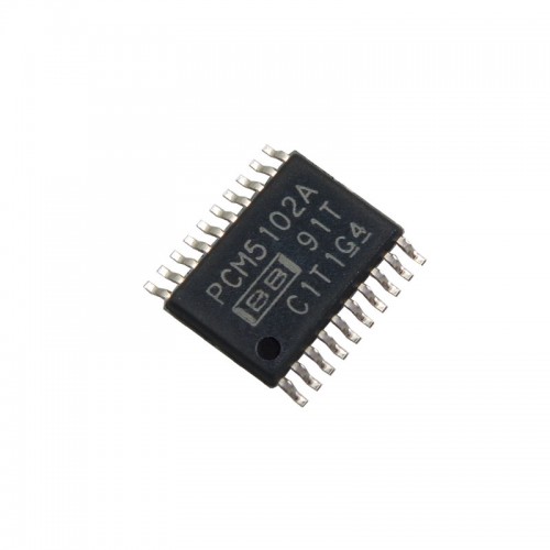
It operates at 16 bits and a sampling frequency that ranges from 8KHz to 384KHz.
It only needs to be fed with the I2S signals, and it doesn’t need a system clock signal.
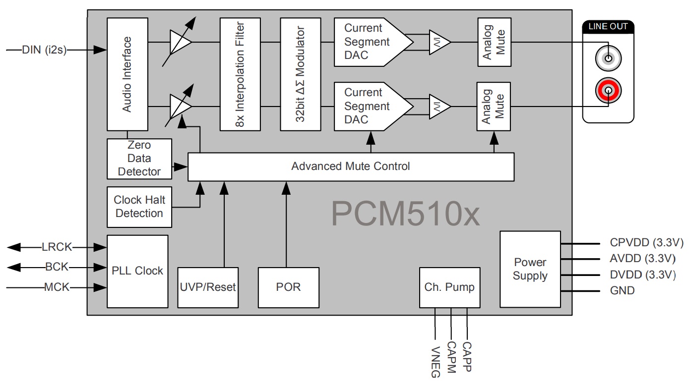
BLOCK DIAGRAM
As with the ADC, this DAC also comes in development boards that will be used in this stage of the project.
I2S and DMA - Ping-Pong buffering
We want our MCU to continuously receive and send digital audio streams in combination with the DAC and ADC. These streams will be transmitted using the I2S interface and the DMA, both peripherals are already integrated in the uC.
I2S (Inter-IC Sound) is a serial communication protocol used for transmitting digital audio data between integrated circuits, commonly found in audio equipment. It consists of three signals, the sample data, word clock, and bit clock.
The DMA (Direct Memory Access) is a peripheral which is used to transfer data between the main memory and the microcontroller peripherals without involving the central processing unit. In this case it will manage the data transfer between the buffers and the I2S interfaces. DMA significantly improves system performance by reducing the CPU’s involvement in data transfer tasks.
DAC Configuration (PCM5102)
Basically, these are the configured parameters in the i2s3 (transmitter):
Parameter settings:
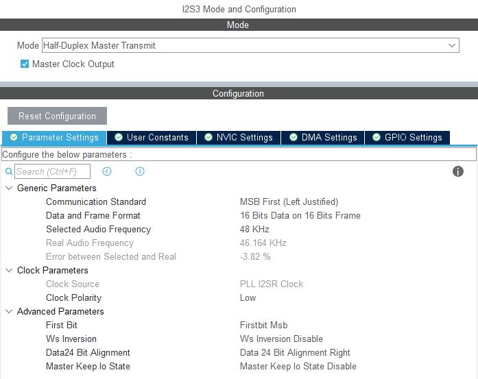
- Mode: Half-Duplex Master Transmit
- Comunication Standard: MSB First (Left Justified)
- Data and Frame Format: 16 bits on 16 Bits Frame
- Selected audio frequency: 48KHz
DMA settings:
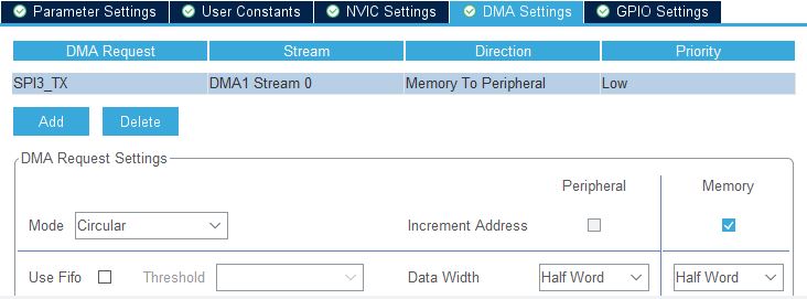
Add a DMA request (SPI3_TX is the default name)
- Stream: DMA1 Stream 0
- Data Width: Half-Word (16bit)
- Direction: Memory To Peripheral
GPIO Settings:
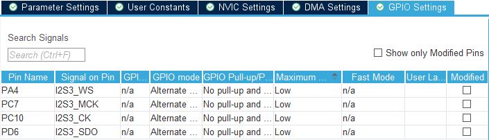
- I2S3_WS (Word select, also known as LeftRightClock)
- I2S3_CK (Clock)
- I2S3_SDO (Data output)
A physical pin of the MCU (PA4, PC7…) needs to be assigned to every signal individually. This is configurable and is usually determined based on the layout of the PCB. It can be changed anytime.
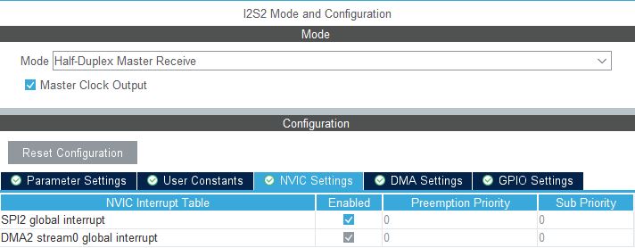
ADC Configuration (PCM1808)
For the receiver, another independent I2S needs to be configured. In this case, it will be the I2S2. As was exposed earlier, the ADC, unlike the DAC, requires a master clock signal to be provided. The rest of the configuration is almost identical, the configured parameters are those:
Parameter settings:
- Mode: Half-Duplex Master Receive
- Master Clock Output (MCO): On
- Comunication Standard: MSB First (Left Justified)
- Data and Frame Format: 24 bits on 32 Bits Frame
- Selected audio frequency: 48KHz
DMA settings: Add a DMA request (SPI2_RX is the default name)
- Stream: DMA2 Stream 0
- Data Width: Word (32bit)
- Direction: Peripheral to Memory
GPIO Settings: In this case we need another signal for the MCO:
- I2S2_WS (Word select, also known as LeftRightClock)
- I2S2_CK (Clock)
- I2S2_SDO (Data output)
- I2S2_MCK (MCO)
Ping-Pong buffering
If we proccess the same data that is being received or transmitted it would probably result in corruption of the data streams. To solve that, a technique called Ping-Pong Buffering is often used in multimedia and real-time systems for smooth data flow.
In a few words, with Ping-Pong Buffering one half of the buffer is being processed while the other half is being written or transmitted, depending on whether it is used for transmision or reception. In this case it is used for both purposes.
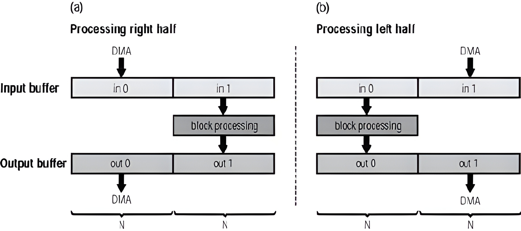
One way to implement this technique is by using callbacks to switch between the two halves of the buffer. By doing that, an interrupt routine will trigger the callback function every time the DMA has transmitted any of the two halves.
NVIC Settings
In order to make those callback functions the NVIC settings must be configured. We need to add an interrupt routine for one DMA stream, which in this case it was decided to be the reception (DMA2 Stream0 and SPI2).
Measuring audio quality
At this point the system is able to receive and transmit audio correctly. It is time to check that the conversion is not introducing artifacts, noises or distortion before implementing actual processing algorithms.
The test procedure consists of measuring the system output when it is fed with a sinusoidal sweep by using the software REW. There will be a set of 8 measurements, 4 of them are the actual output of the DAC at various input volume levels and the other 4 are the control measurements.
Those control measurements are made with the same output volume and input gain than each of the real measurements but, instead of feeding the input of the ADC with the output of the soundcard, the input of the soundcard will be connected to its own output without any intervention of the DSP (loopback). This is done to avoid wrong conclussions about audio problems that may be caused by the soundcard and not the DSP.
Frequency response
In this measurement it can be seen that all the control measurements give essentially the same result, except the fact that the high pass filter at 10Hz has a higher cutoff frequency when the volume is set too low. This is because there is an analog high pass filter on the output of the soundcard to which the load is the input of the soundcard (because there is a loopback) and, when the potentiometer at the input is changed, the transfer function of this filter also changes.
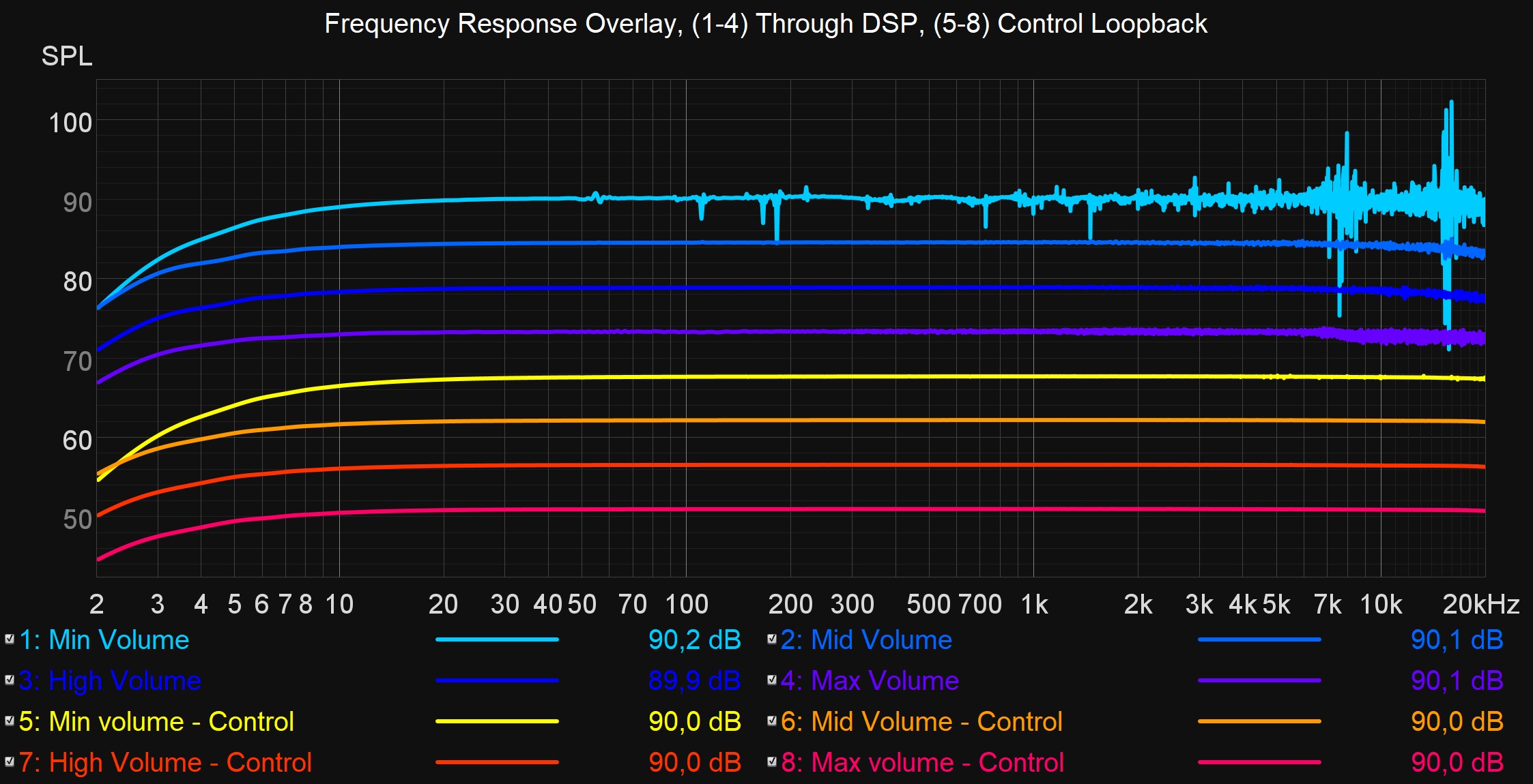
Apart from that, we can also see that all the DSP measurements are coherent in its SPL over all the audible frequencies. Despite that, there are clearly some problems on the minimum and maximum volume measurements, especially at the highest frequencies.
Total Harmonic Distortion (THD) + Noise floor
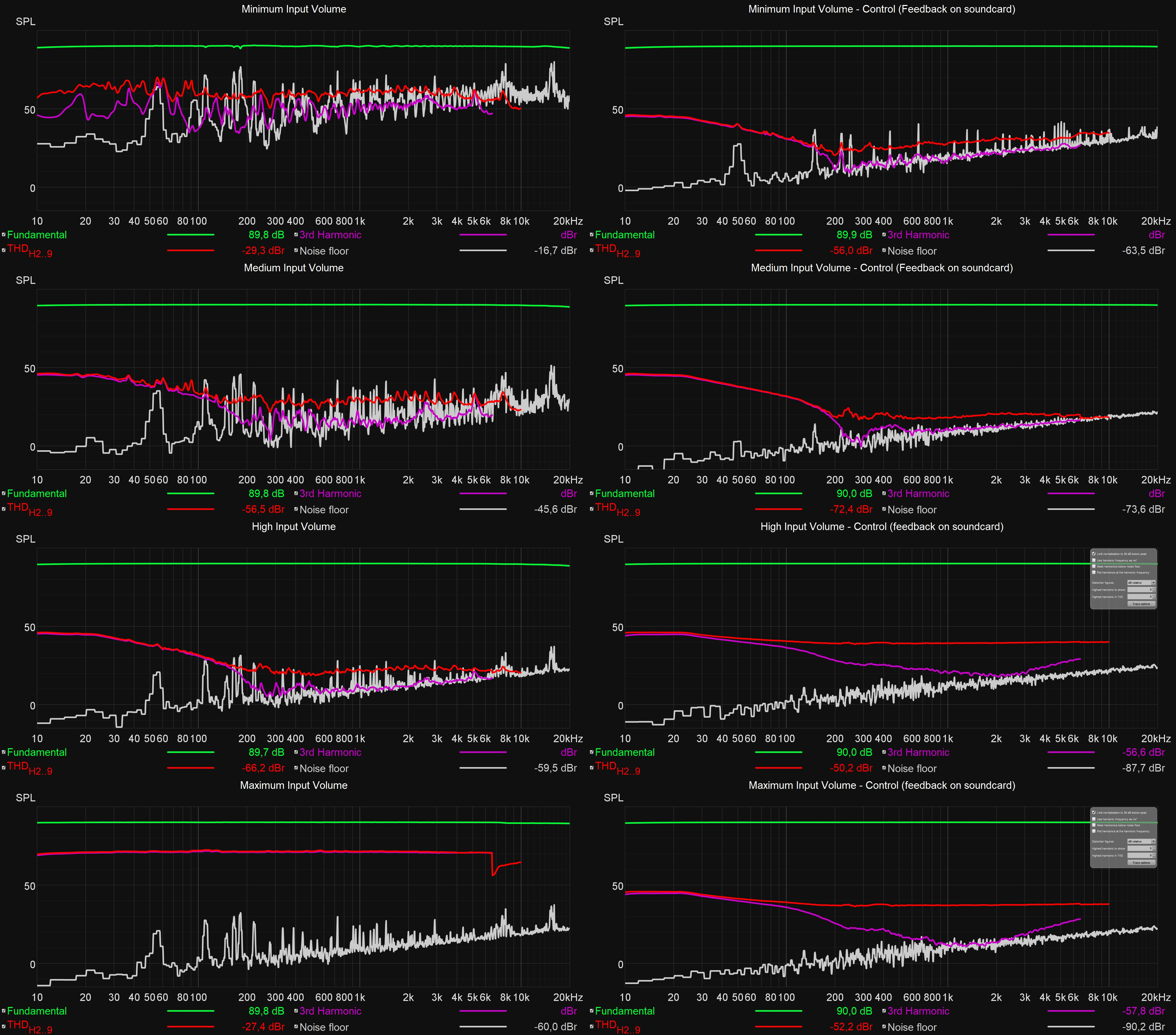
It can clearly be seen that, as the input volume increases there is less noise floor. This is supposed to happen because the whole amplitude of the signal is being sampled with less bit depth, which increases noise.
In addition, when the input volume increases too much, the ADC saturates and adds distortion to the signal. We can see how the THD increases massively on the maximum volume measurement which, as will be exposed below, caused ADC saturation.
Conclussions on this measurement
- It is important to have an adequate input level to reduce noise floor.
- We have to avoid exceeding the maximum amplitude range of the ADC.
- Although the noise floor levels are not too bad, there is room for improvement.
It is expected for the performance of the conversions to be improved by applying a few DSP techniques as monitoring the ADC limit or increasing the sampling frequency and adding a decimation filter after the ADC stage.
Captured signal
Medium-high Volume
The signal at normal volumes seems to be clean.
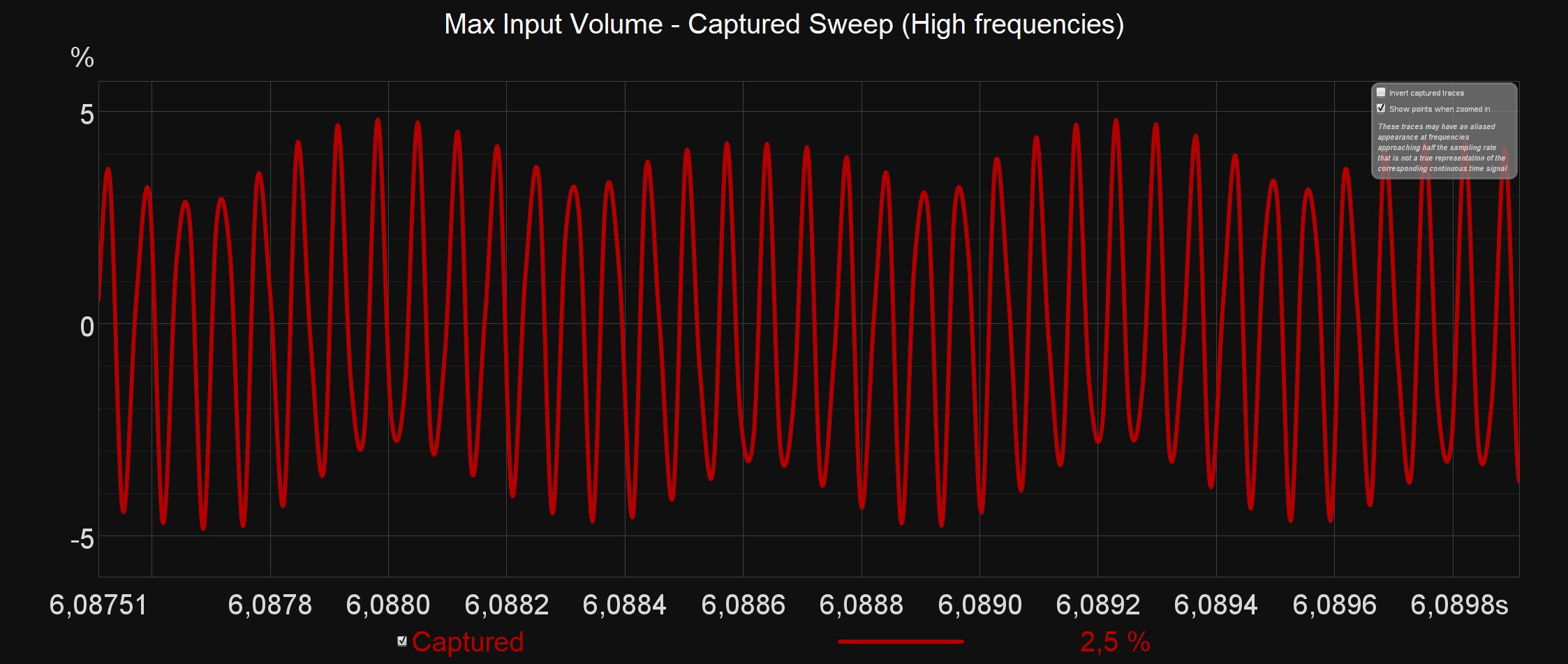
Max Volume
The first problem that can be seen is the distortion that we noticed earlier. When the signal amplitude exceeds the dynamic range of the ADC it saturates as can be seen in the image below. This was expected but can be avoided in many different ways.
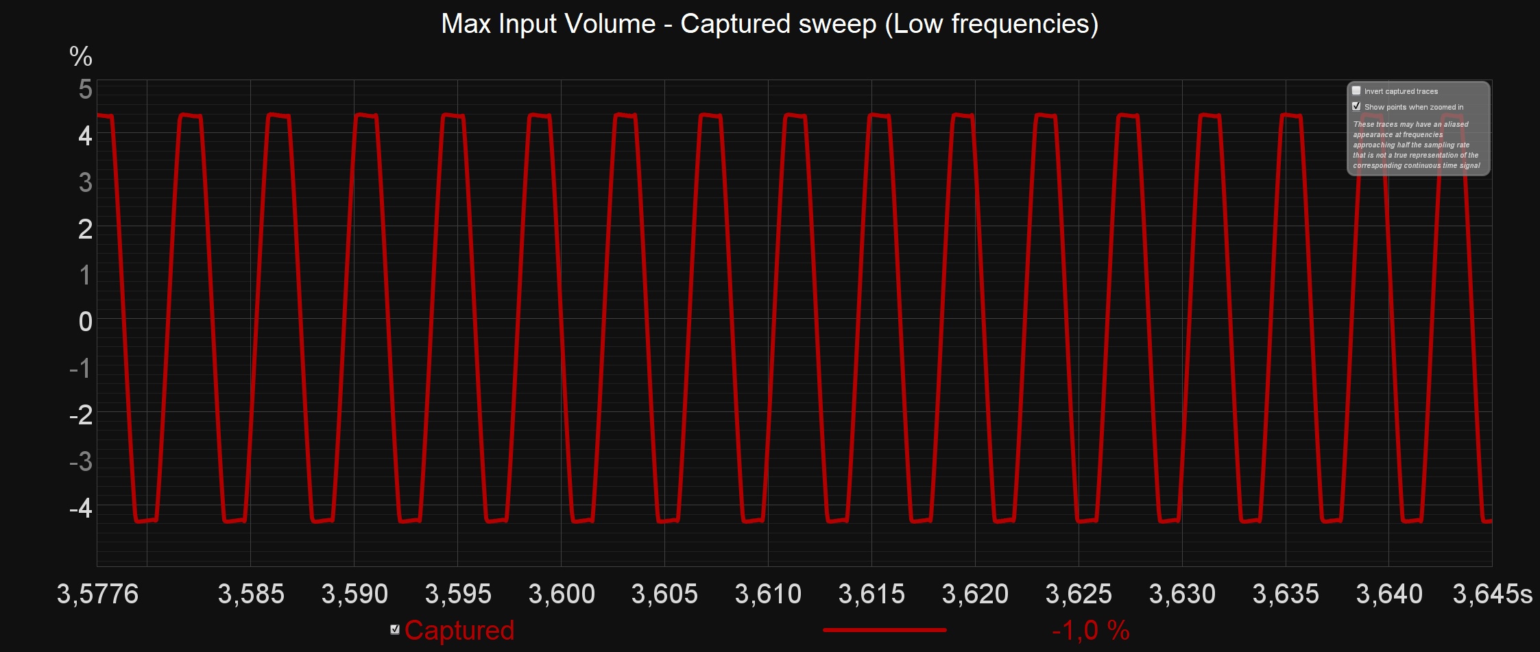
Another problem that may be the formation of aliasing at high frequencies. This might be the reason why there is a less linear drequency response and an increased floor noise at high frequencies.
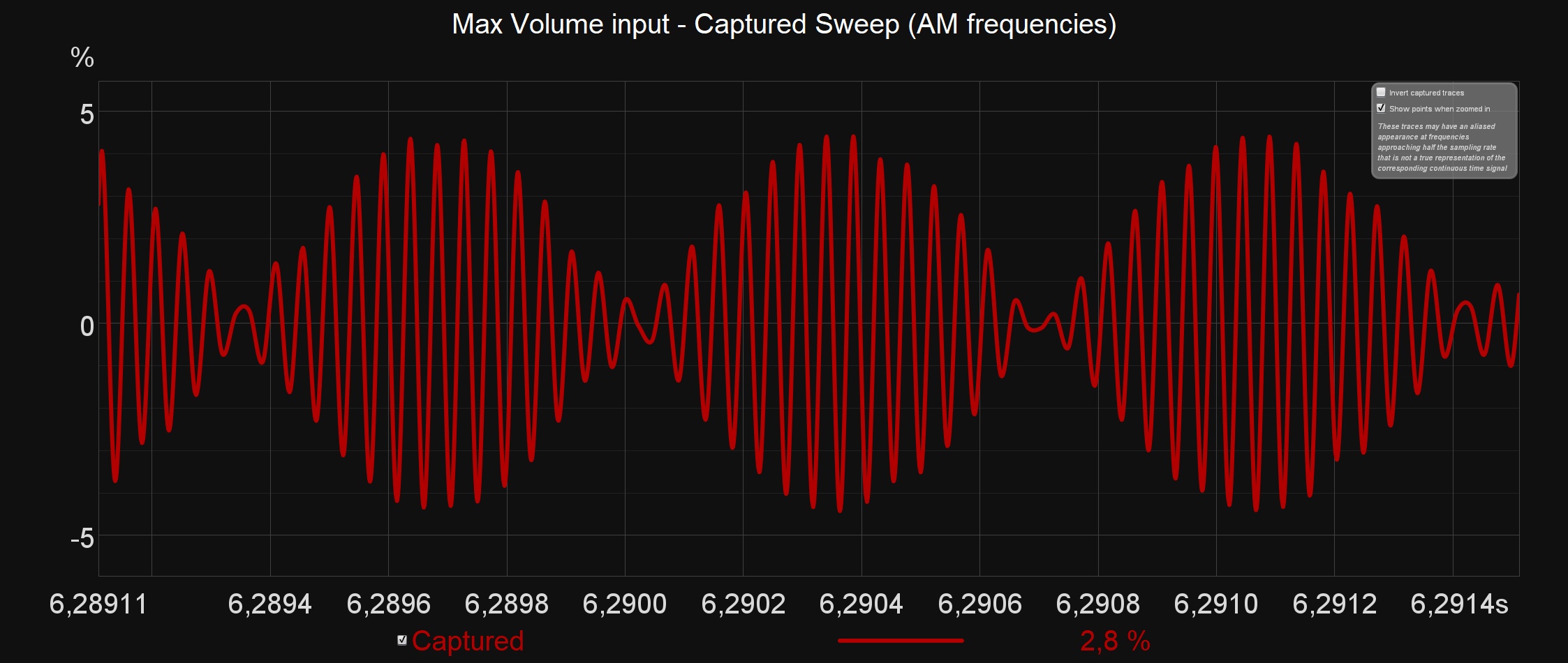
Below we can also see that, at some determined frequencies this aliasing is causing an amplitude modulation.
Delay
The delay of the system was measured with the oscylloscope. A low frequency square wave was introduced to the system and then the time difference between the output and input flancs was measured. This time difference represents the delay of the system.
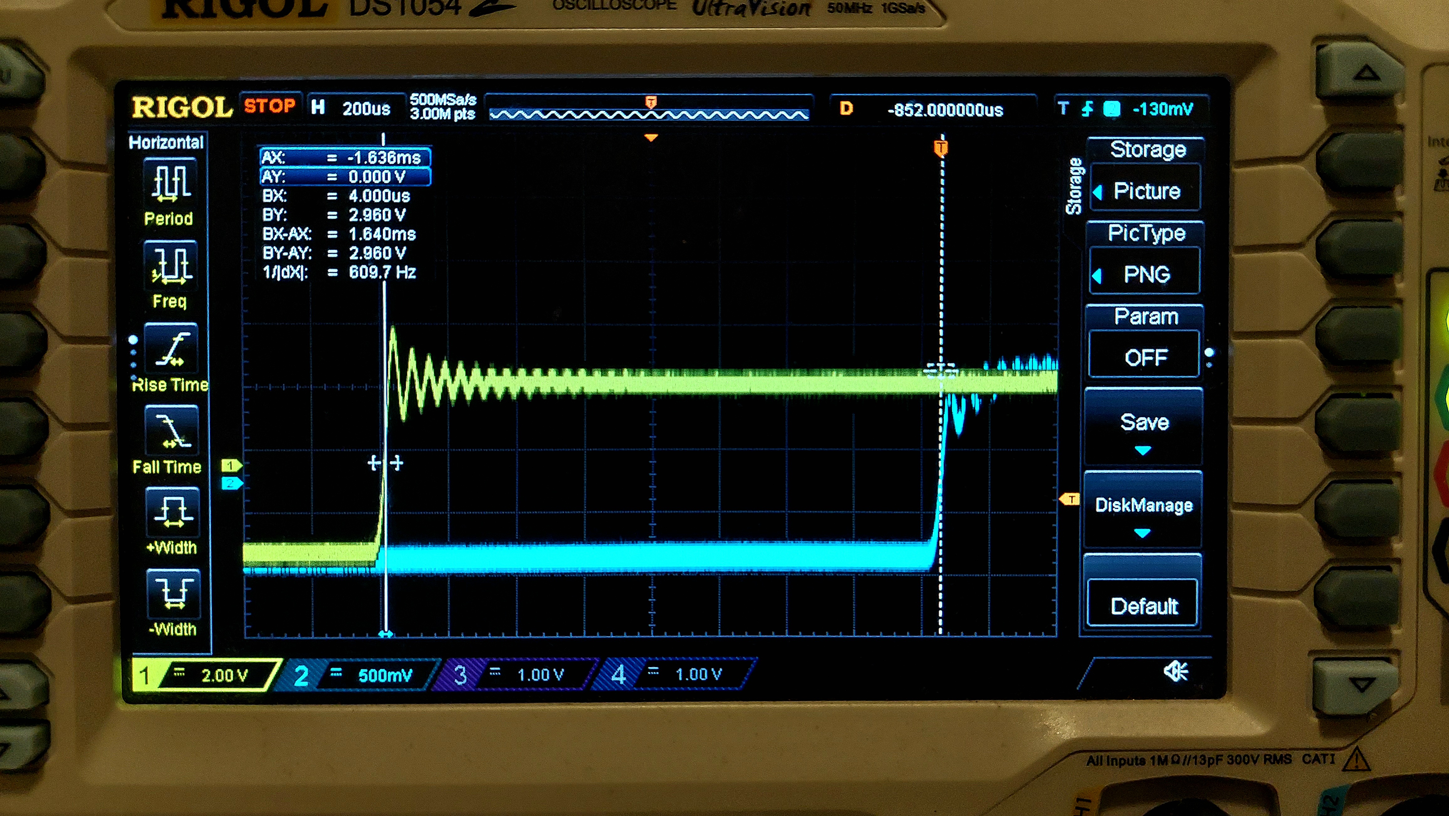
As we can see, the delay is 1.636ms, which makes sense because we are using a buffer size of 64 samples with a sampling frequency of 48KHz, which results in a base delay of 1.3ms. The other 0.3ms may be caused by the extra processing involved in copying the samples from the input buffer to the output buffer.