
Introduction
Vibratio is an intuitive, modular, and efficient DSP platform with a focus on advanced audio processing techniques and connectivity options for real-time audio product development. With its high flexibility, this platform empowers the creation of complex projects such as portable speakers, synthesizers, and noise-cancelling systems.
The objective is to create an industry-standard platform which enables future projects to reach the technology level of the most powerful audio products in the market.
This project explores various disciplines, including advanced DSP techniques for audio, communication protocols, buffering, data streaming, hardware design, and software optimization for power efficiency.
System Overview
The system is a microcontroller-based solution designed to handle both digital and analog audio inputs, capable of processing audio sources using customizable DSP algorithms.
The PCB includes peripherals and connectors to meet the following connectivity requirements:
- Bluetooth A2DP, aptX
- Line input
- Preamplified input (for instruments)
- Stereo Line output
- Stereo auxiliary output (for 2.1 speaker systems)
- Battery connection
- USB connection for external programming and/or battery charging
The device can disable unused peripherals to reduce power consumption in future projects.
Block Diagram
The following diagram illustrates the system architecture. The yellow rectangle represents the complete hardware device, including the microcontroller and ICs for A/D and D/A conversion. The blue rectangle represents the microcontroller, with internal blocks consisting of digital algorithms and communication protocols.
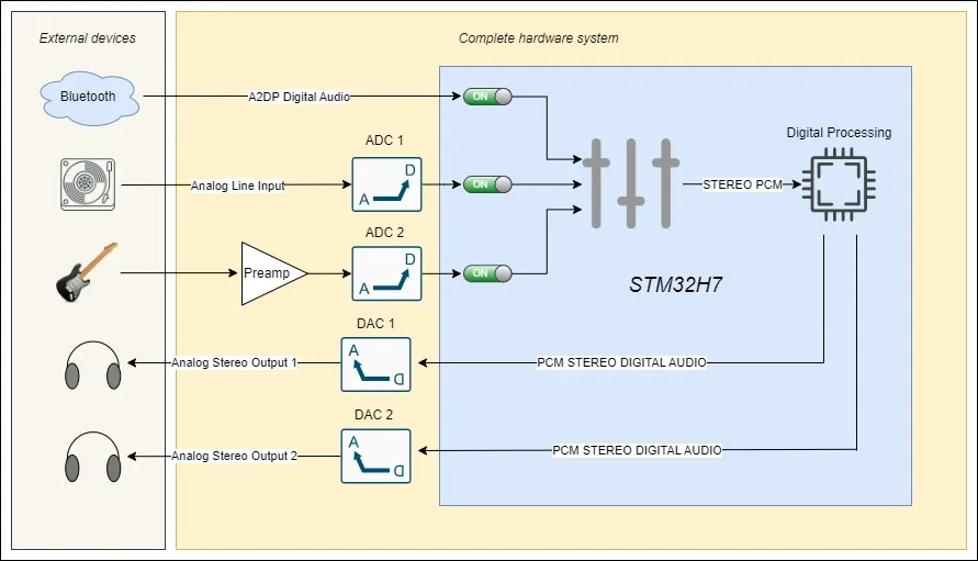 Figure 1. System block diagram
Hardware Overview
The hardware components include:
- Bluetooth receiver
- 2x Stereo ADCs
- 2x Stereo DACs
- Preamplification circuit
Note: The bluetooth and instrument inputs are still being developed. This documentation currently covers the line input (ADC1) and main output (DAC1) implementation, which are fully operational.
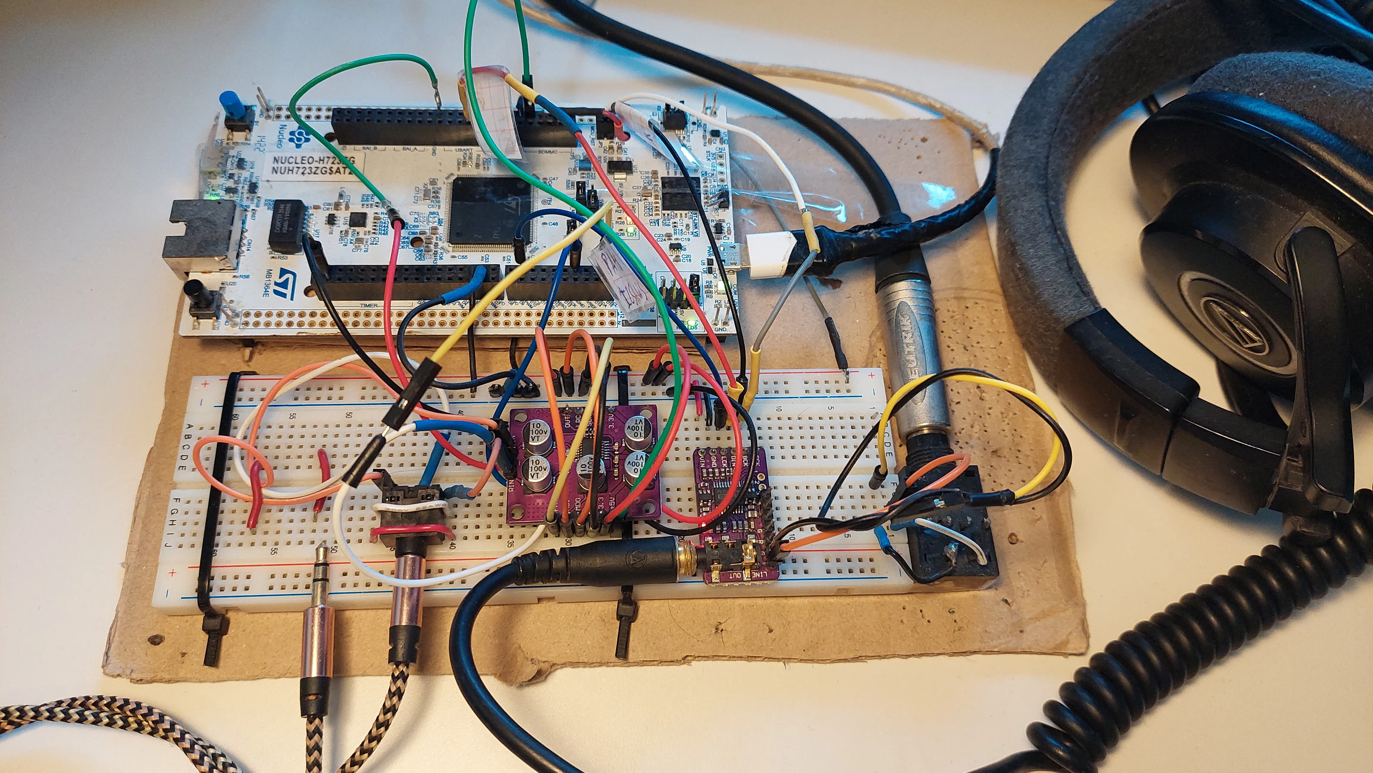 Figure 2. System hardware components
A/D Converters
The chosen IC for A/D conversion is the PCM1808 from Texas Instruments.
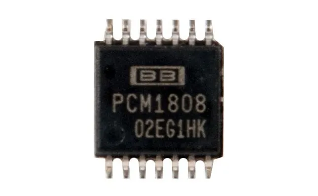 Figure 3. PCM1808 from Texas Instruments
It is a single-ended stereo ADC that operates at 24 bits with a sampling frequency ranging from 44.1 to 96 KHz depending on clock configuration. The converted audio streams via the I2S protocol.
Built-in features:
- Oversampling Decimation Filter (prevents aliasing noise)
- On-Chip Analog Low-Pass Filter
- On-Chip High-Pass Filter
- Power Down and Reset System
- Configurable I2S format
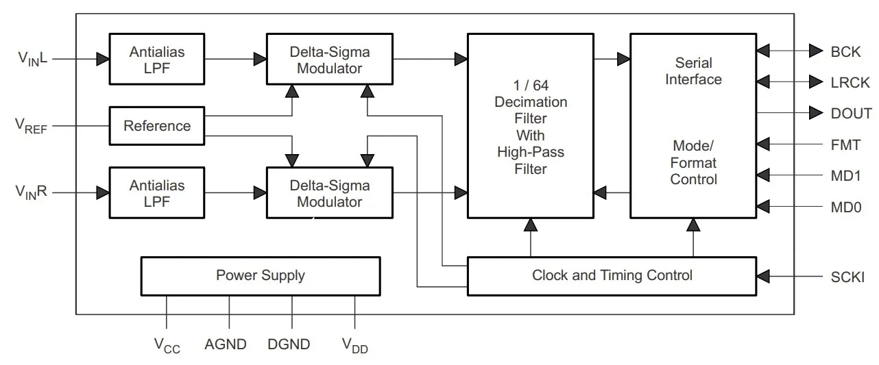 Figure 4. PCM1808 Block Diagram
The IC requires a synchronized System Clock signal along with the I2S signals. For early development, a PCM1808 development board is used:
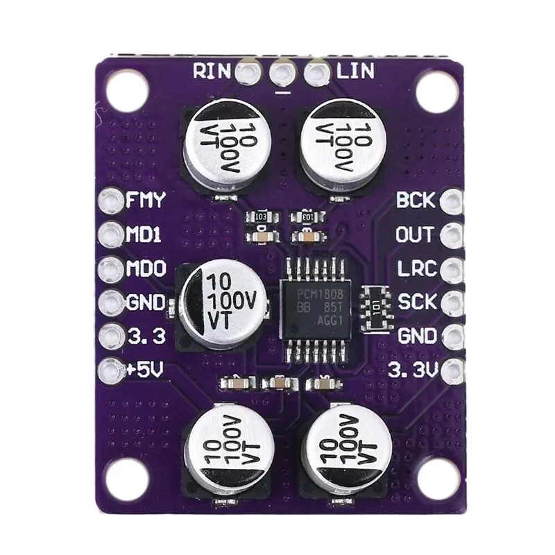 Figure 5. PCM1808 development board
D/A Converters
The digital-to-analog conversion uses the PCM5102 from Texas Instruments—a simple but effective IC used in previous projects.
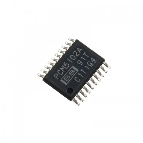 Figure 6. PCM5102 from Texas Instruments
It operates at 16 bits with a sampling frequency ranging from 8KHz to 384KHz. It requires only I2S signals and does not need a separate system clock signal.
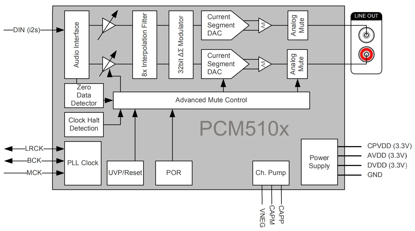 Figure 7. PCM5102 Block Diagram
The DAC is also available in a development board:
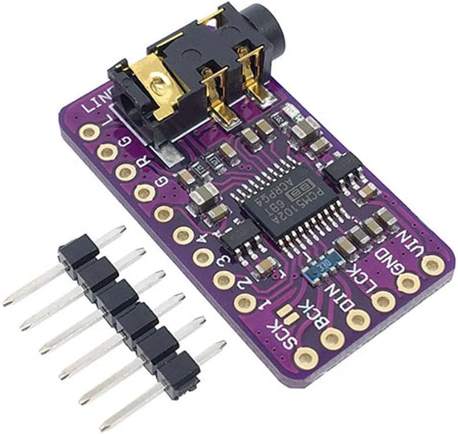 Figure 8. PCM5102 development board
I2S and DMA - Ping-Pong Buffering
The MCU continuously receives and sends digital audio streams via the I2S interface and DMA, both integrated into the microcontroller.
I2S (Inter-IC Sound) is a serial communication protocol for transmitting digital audio data between ICs. It consists of three signals: sample data, word clock, and bit clock.
DMA (Direct Memory Access) transfers data between main memory and MCU peripherals without CPU involvement. It manages data transfer between buffers and I2S interfaces, significantly improving system performance.
DAC Configuration (PCM5102)
I2S3 Parameter Settings:
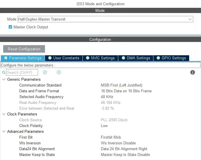 Figure 9. I2S3 Parameter Configuration
- Mode: Half-Duplex Master Transmit
- Communication Standard: MSB First (Left Justified)
- Data and Frame Format: 16 bits on 16 Bits Frame
- Selected Audio Frequency: 48KHz
DMA Settings:
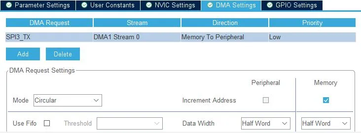 Figure 10. I2S3 DMA Configuration
- Stream: DMA1 Stream 0
- Data Width: Half-Word (16bit)
- Direction: Memory To Peripheral
GPIO Settings:
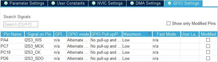 Figure 11. I2S3 GPIO Configuration
I2S protocol signals:
- I2S3_WS (Word select / LeftRightClock)
- I2S3_CK (Clock)
- I2S3_SDO (Data output)
Physical pins are assigned based on PCB layout and can be reconfigured.
ADC Configuration (PCM1808)
The ADC uses I2S2 and requires a master clock signal. Configuration is similar to the DAC with these parameters:
Parameter Settings:
- Mode: Half-Duplex Master Receive
- Master Clock Output (MCO): On
- Communication Standard: MSB First (Left Justified)
- Data and Frame Format: 24 bits on 32 Bits Frame
- Selected Audio Frequency: 48KHz
DMA Settings:
- Stream: DMA2 Stream 0
- Data Width: Word (32bit)
- Direction: Peripheral to Memory
GPIO Settings:
- I2S2_WS (Word select)
- I2S2_CK (Clock)
- I2S2_SDI (Data input)
- I2S2_MCK (Master Clock)
Important: Both I2S interfaces must be triggered by the same clock source for synchronous operation. I2S2 and I2S3 share the same PLL clock source, ensuring identical sampling frequencies. The MCO is enabled for I2S3 to ensure both interfaces are multiplexed to the same PLL clock.
Ping-Pong Buffering
Processing the same data being received or transmitted would corrupt the data streams. Ping-Pong Buffering is a technique used in real-time systems for smooth data flow.
One half of the buffer is processed while the other half is being written or transmitted. This applies to both reception and transmission.
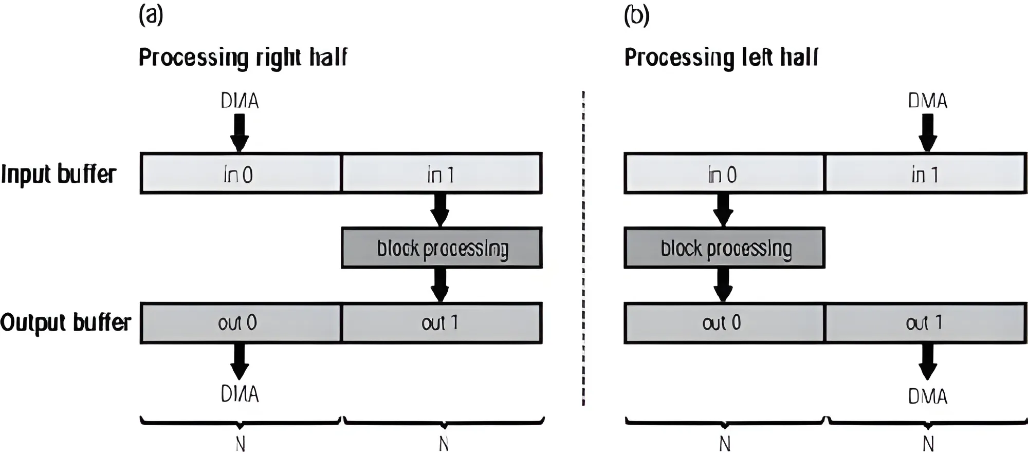 Figure 12. Ping-Pong Buffering Technique
Implementation: Callbacks switch between buffer halves. An interrupt routine triggers the callback every time the DMA completes a half-buffer transfer.
NVIC Settings:
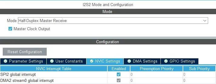 Figure 13. I2S2 NVIC Configuration
An interrupt routine is configured for the reception DMA stream (DMA2 Stream0 / SPI2).
Measuring Audio Quality
With the system receiving and transmitting audio correctly, it’s time to verify that conversion doesn’t introduce artifacts, noise, or distortion before implementing DSP algorithms.
Test Procedure
The system output is measured when fed with a sinusoidal sweep using REW software. Eight measurements are taken:
- 4 DSP measurements: Actual DAC output at various input volume levels
- 4 control measurements: Loopback connections (soundcard output to input) at matching volumes
Control measurements identify issues caused by the soundcard versus the DSP.
Frequency Response
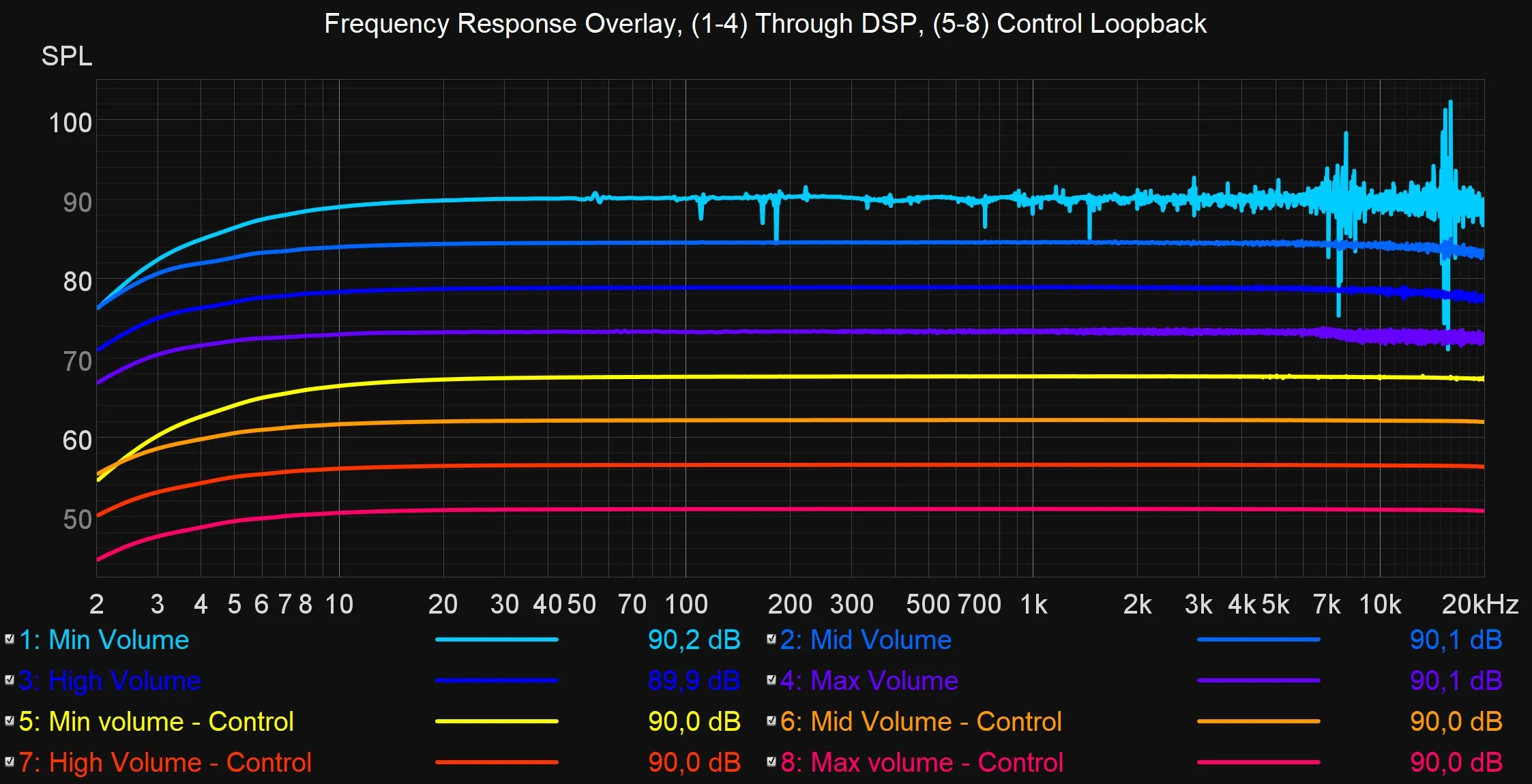 Figure 14. Frequency response test
All control measurements are essentially identical, except the high-pass filter at 10Hz has a higher cutoff frequency at minimum volume due to the analog output filter’s transfer function changing with input potentiometer settings.
DSP measurements show coherent SPL across audible frequencies. However, problems appear at minimum and maximum volumes, especially at high frequencies.
Total Harmonic Distortion (THD) + Noise Floor
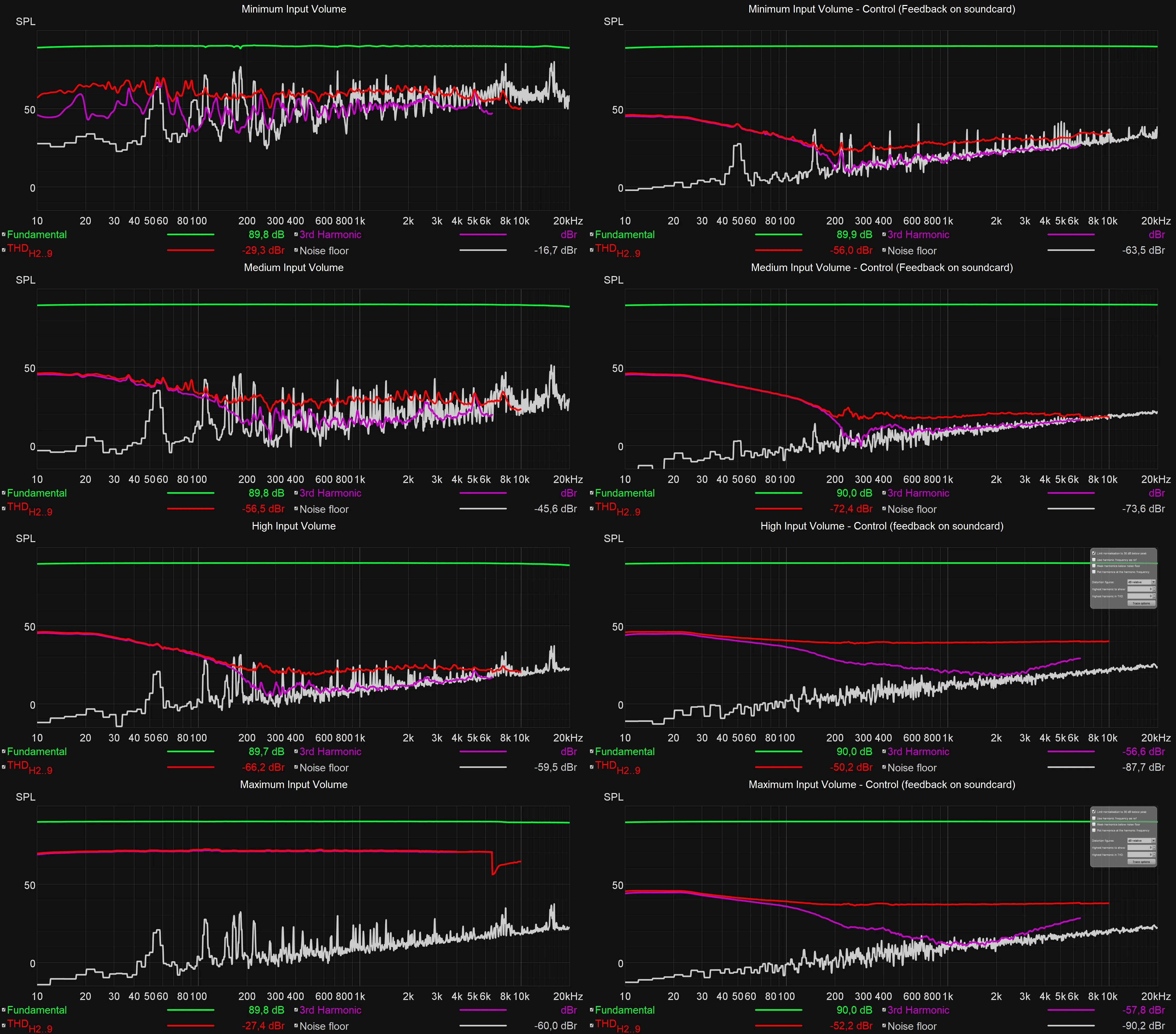 Figure 15. THD + Floor Noise at 4 different input volumes
As input volume increases, noise floor decreases. This is expected—lower volumes result in reduced bit depth for signal sampling, increasing noise.
When input volume is too high, ADC saturation adds significant distortion. THD increases massively at maximum volume due to saturation.
Conclusions:
- Adequate input level is important to reduce noise floor
- Avoid exceeding the ADC’s maximum amplitude range
- Noise floor levels are acceptable but can be improved
Performance improvements can be achieved through DSP techniques like ADC monitoring, increased sampling frequency, and decimation filtering.
Captured Signal
Medium-High Volume
The signal at normal volumes appears clean.
Max Volume
Problem 1: Saturation
When signal amplitude exceeds the ADC’s dynamic range, saturation occurs:
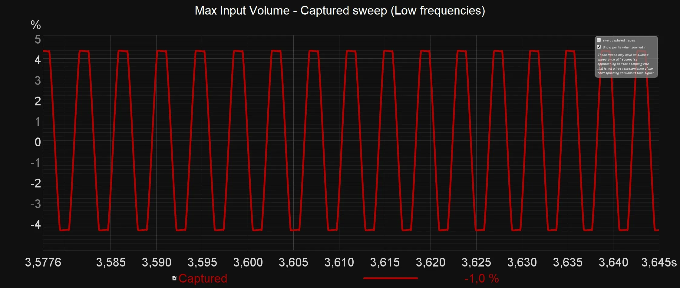 Figure 16. Saturated signal at max volume
Problem 2: Aliasing at High Frequencies
Aliasing may be causing less linear frequency response and increased noise floor at high frequencies:
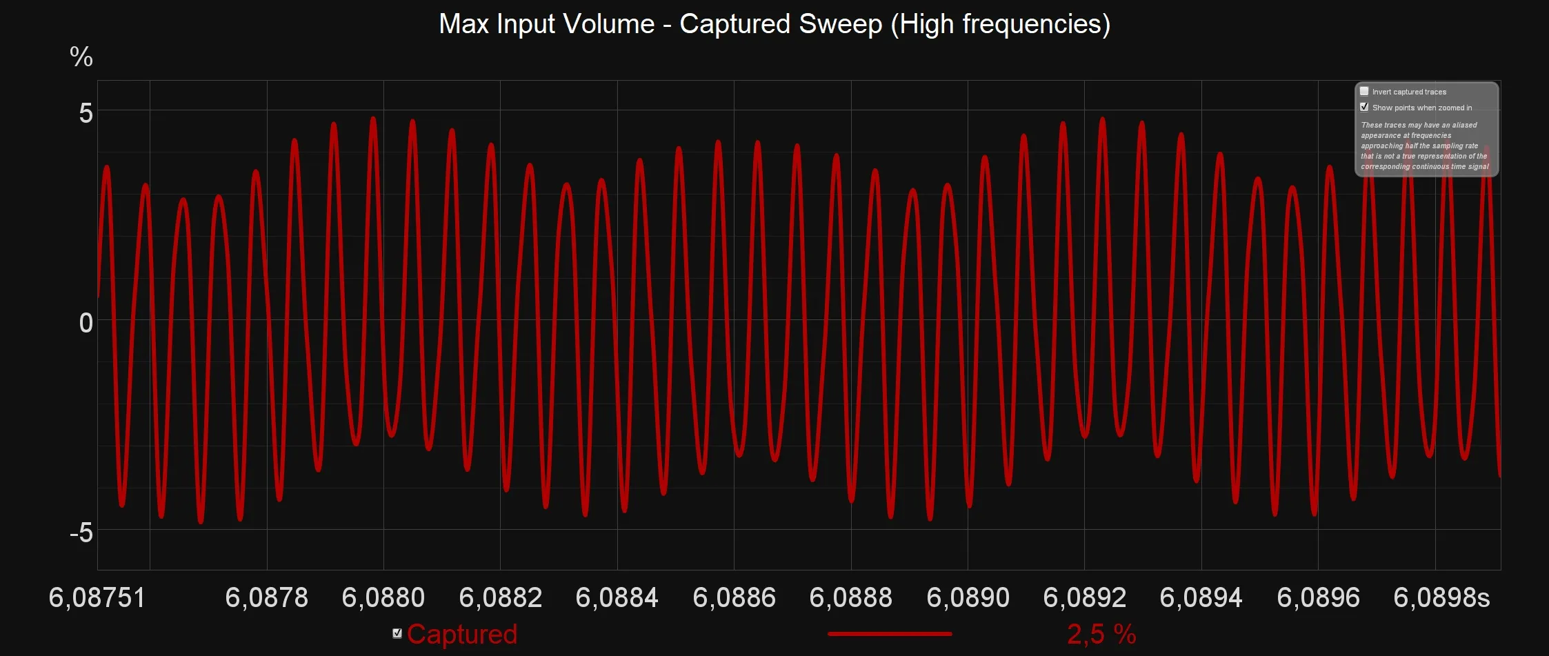 Figure 17. Aliasing effect at high frequencies
At certain frequencies, aliasing causes amplitude modulation:
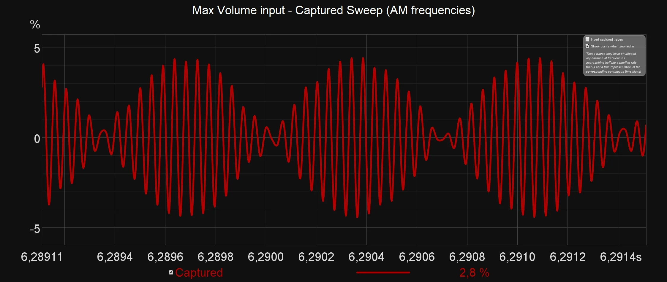 Figure 18. Amplitude modulation caused by aliasing
Delay
System delay was measured with an oscilloscope. A low-frequency square wave was input, and the time difference between output and input flanks was measured.
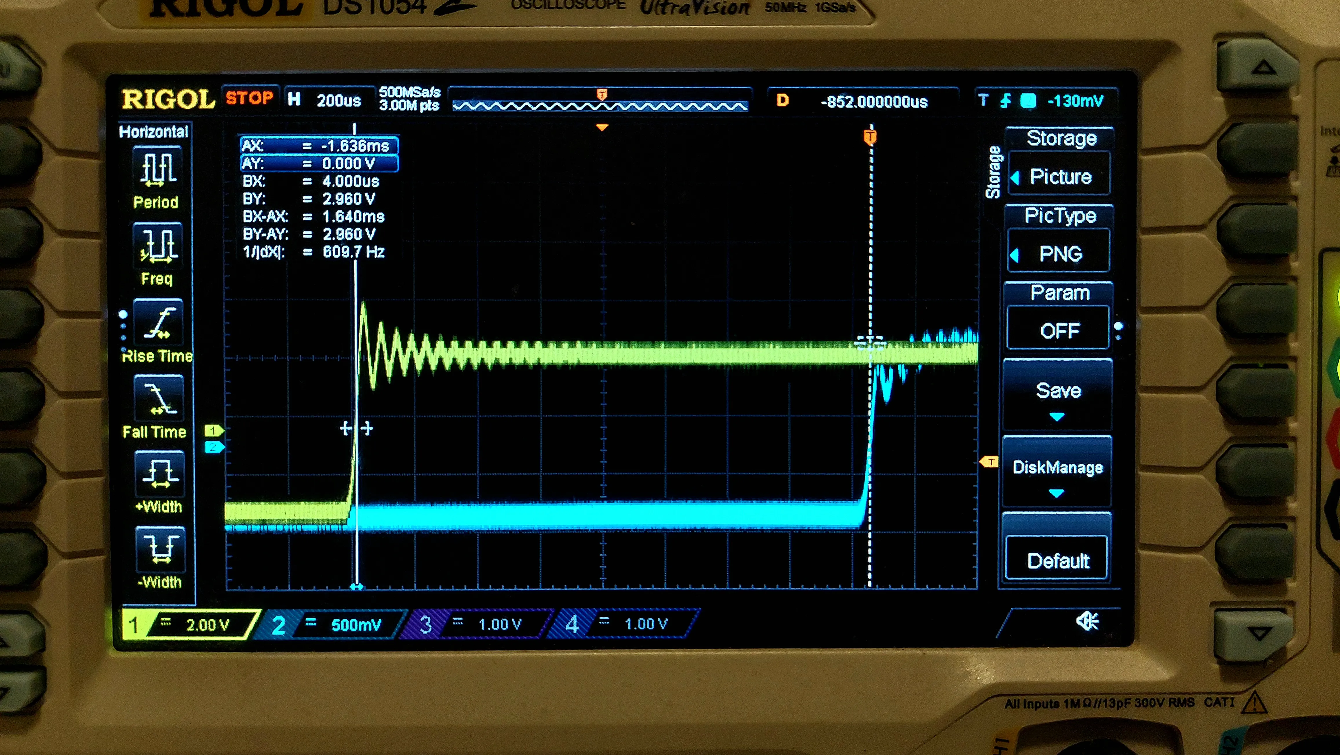 Figure 19. Delay measurement using oscilloscope
Measured delay: 1.636ms
This is consistent with a buffer size of 64 samples at 48KHz sampling frequency, resulting in a base delay of 1.3ms. The additional 0.3ms is likely due to processing overhead in copying samples from input to output buffers.
Future Development
The project continues to evolve with plans for:
- DSP algorithm implementation (filters, dynamics, effects)
- Bluetooth integration (A2DP, aptX)
- Instrument preamp circuit
- Full-system mixed-signal PCB design
- Power optimization
- Advanced noise reduction techniques
Technical Specifications
| Parameter | Value |
|---|---|
| Microcontroller | STM32H7 series |
| ADC Resolution | 24-bit |
| DAC Resolution | 16-bit |
| Sampling Rate | 48 kHz |
| Buffer Size | 64 samples |
| System Latency | 1.636 ms |
| Communication | I2S (Left Justified) |
| Data Transfer | DMA (Ping-Pong Buffering) |
This project represents a comprehensive foundation for professional-grade audio DSP applications, combining hardware design, real-time processing, and signal integrity measurement.